Difference between revisions of "Microfluidics"
From mn.fysikk.laglivlab
Dagkd@uio.no (talk | contribs) |
Dagkd@uio.no (talk | contribs) |
||
| Line 19: | Line 19: | ||
= Photolithography = | = Photolithography = | ||
| − | [https://wiki.uio.no/mn/fysikk/laglivlab/index.php/Photolithography | + | [https://wiki.uio.no/mn/fysikk/laglivlab/index.php/Photolithography Photolithography procedures] |
= PDMS casting = | = PDMS casting = | ||
Revision as of 11:50, 3 April 2022
Contents
Designing Microfluidic masks
- Stanford microfluidics foundry has a good guide for designing your own device. That includes a guide to use AutoCAD.
- AutoCAD (a program from Autodesk) is available free.
- You can use Klayout but we have more support for using Autocad.
- Mask template for placing your designs
- This guide for designing masks has some important tips
- All fluid pathways have to be inside one or more closed contour(s)
- The outer contour should be drawn in one layer (Give it a name like "Flow")
- Any obstacles inside this outer contour must be drawn in another layer. Give it a name like "Flow inner polygons")
- Displaying your design as PDF or otherwise is not straight forward because the resolution needed. You get a fair impression using CloudConvert which is much better than AutoCads own pdf export.
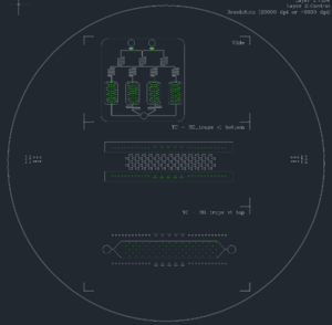
- Example of a design where white lines (in screen shot below, black lines in PDF) are contours containing flow and green lines are inner polygons. Here is a PDF version of the file and the DWG file.
- Rounding corners on a region
- Command EXPLODE makes region into lines
- Command JOIN joins lines into polylines
- Command FILLET, downarrow to get options RADIUS and POLYLINE
