Difference between revisions of "Mathias' process"
Dagkd@uio.no (talk | contribs) (start) |
Dagkd@uio.no (talk | contribs) (put in tables) (Tag: Visual edit) |
||
| Line 68: | Line 68: | ||
21. If particles are remaining, put back in PGMEA for 2-3 min, rinse with IP and dry with nitrogen. Redo until fully developed. | 21. If particles are remaining, put back in PGMEA for 2-3 min, rinse with IP and dry with nitrogen. Redo until fully developed. | ||
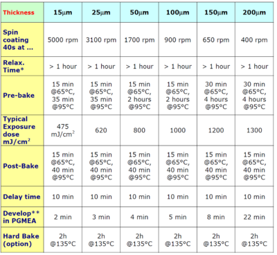
| + | [[File:GM1070params.png|left|thumb|400x400px|Process parameters for different thicknesses of GM 1070]] | ||
| + | {| class="wikitable" | ||
| + | |+Exposure dose of UV KUB 2 measured with dosimeter (2020) for 1000% power | ||
| + | !Exposure time [s] | ||
| + | !1 | ||
| + | !2 | ||
| + | !5 | ||
| + | !10 | ||
| + | !20 | ||
| + | !30 | ||
| + | |- | ||
| + | |Dose [mJ/cm<sup>2</sup>] | ||
| + | |45 | ||
| + | |93 | ||
| + | |235 | ||
| + | |469 | ||
| + | |901 | ||
| + | |1330 | ||
| + | |} | ||
Revision as of 16:14, 8 March 2021
Protocol SU-8 master fabrication (Mathias Busek 2020)
Materials: GM 1070 (SU-8), PGMEA (Developer), 4-inch Si Wafer (Substrate), IP
Tools: Clean bench, Spin-Coater, Hotplate, UV exposer (UV KUB 2), wafer tweezer, wafer holder for development, nitrogen gun, spray bottle, beakers
Preparation:
1. Turn on clean bench and remove cover.
2. Turn on nitrogen valve.
3. Turn on vacuum for spin-coater (use small mobile pump or big pump at the entrance).
4. Close doors and windows and turn on yellow light in both rooms and the hood.
5. Under the hood:
a. Poor PGMEA in a big glass tank for development.
b. Clean a second beaker for washing the wafer.
c. Fill a spray bottle with IP.
Fabrication:
1. Clean wafer (if is not clean, e.g. using plasma cleaner, acetone and IP). Dry with nitrogen.
2. Dry wafer on hot plate for at least 10 min at 150 degree and cool down.
3. Poor enough SU-8 on wafer, distribute by hand and use needle to destroy bigger bubbles.
4. Align on spin-coater (centric)
5. Spin for at least 40s on about 200 rpm and another 40s of rate according to table 1.
6. Rest on spin-coater for at least 15 min, better one hour.
7. Put on hotplate and heat-up to 65 degree.
8. Bake for 15/30 min according to table 1.
9. Heat-up to 95 degree and bake according to table 1 (>35 min).
10. Cool down and transfer to exposure system, put mask with printed side down on top of the wafer and glass substrate on the upper side of the tray.
11. Start masking mode and type in substrate thickness (Si wafer 630 um) + thickness of your layer.
12. Set exposure time according to dose given on table 2 (for small structures use 50% or less of the exposure dose given in the table). One can also split exposure dose in smaller cycles e.g. 2 x 10s instead of 20s. The measured
intensity is given in table 2. (UV KUB 2 has approx. 40 mW/cm2.)
13. Press insulate to expose.
14. Remove wafer from tray and let rest for at least 10 min.
15. Put on hotplate and heat-up to 65 degree.
16. Bake for 15 min at 65 degree and 40 min at 95 degree.
17. Cool wafer down and fix in holder for development.
18. Transfer to hood (be sure to turn off all white light) and put in PGMEA bath.
19. Develop according to time given in table 1.
20. Immediately rinse with IP and dry with nitrogen.
21. If particles are remaining, put back in PGMEA for 2-3 min, rinse with IP and dry with nitrogen. Redo until fully developed.
| Exposure time [s] | 1 | 2 | 5 | 10 | 20 | 30 |
|---|---|---|---|---|---|---|
| Dose [mJ/cm2] | 45 | 93 | 235 | 469 | 901 | 1330 |
